
Wiring is an important part of PCB design, and it is also the most workload-intensive and time-consuming part of the entire PCB design. Engineers need to follow some basic rules when performing PCB wiring work, such as chamfering rules, 3W rules, etc.
Ground loop rules
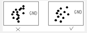
The minimum loop rule means that the loop area formed by the signal line and its loop should be as small as possible. The smaller the loop area, the less external radiation and the smaller the external interference received. In response to this rule, when dividing the ground plane, the distribution of the ground plane and important signal traces must be considered to prevent problems caused by ground plane slotting; in double-layer board design, leave enough space for the power supply. In this case, the remaining part should be filled with reference ground, and some necessary ground vias should be added to effectively connect the double-sided ground signals. Ground wire isolation should be used as much as possible for some key signals, and some higher frequency signals should be isolated. In the design, special consideration must be given to the ground plane signal loop problem, and it is recommended to use a multi-layer board.
Block protection rules
Corresponding to the ground loop rules, it is actually to minimize the loop area of the signal. It is more common in some more important signals, such as clock signals and synchronization signals. For some particularly important and high-frequency signals, copper axis cables should be considered. The shielding structure design is to isolate the laid lines with ground wires, and also consider how to effectively combine the shielding ground with the actual ground plane.
Crosstalk control rules
Crosstalk refers to the mutual interference between different networks on the PCB caused by long parallel wiring, mainly due to the distributed capacitance and distributed inductance between parallel lines. The main measures to overcome crosstalk are:
Increase the spacing between parallel wiring and follow the 3W rule;
Insert grounded isolation wires between parallel wires;
Reduce the distance between wiring layers and ground planes.
3W rule
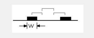
In order to reduce crosstalk between lines, the line spacing should be ensured to be large enough. When the line center spacing is not less than 3 times the line width, 70% of the electric field can be maintained without interfering with each other, which is called the 3W rule. If you want to achieve 98% electric field without mutual interference, you can use a spacing of 10W.
Routing direction control rules
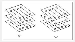
The direction control rules of the traces, that is, the trace directions of adjacent layers form an orthogonal structure. Avoid running different signal lines in the same direction on adjacent layers to reduce unnecessary inter-layer interference; when it is difficult to avoid this situation due to board structure limitations (such as some backplanes), especially when the signal rate is high, Consider using ground planes to isolate wiring layers and ground signal lines to isolate signal lines.
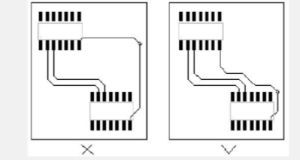
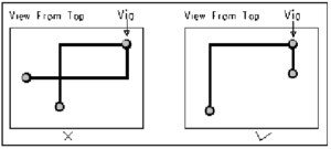
Open-loop inspection rules for wiring
Generally, wiring with one end floating (Dangling Line) is not allowed, mainly to avoid the “antenna effect” and reduce unnecessary interference radiation and reception, otherwise it may bring unpredictable results.
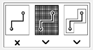
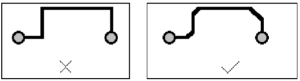
Cabling closed-loop inspection rules
Prevent signal lines from forming self-loops between different layers. Such problems are prone to occur in multilayer board designs, and self-loops will cause radiated interference.
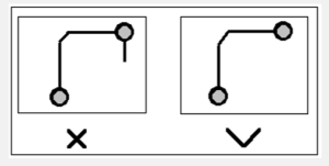
chamfer rules
Sharp angles and right angles should be avoided in PCB design, which will produce unnecessary radiation and poor process performance.
Device decoupling rules
Add necessary decoupling capacitors to the printed plate to filter out interference signals on the power supply and stabilize the power supply signal. It is recommended that the power supply is connected to the power pin through the filter capacitor.
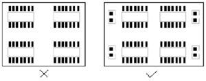
Power Ground Plane Integrity Rules
For areas with dense via holes, care should be taken to avoid holes connecting to each other in the hollowed-out areas of the power supply and ground layers, forming a division of the plane layer, thereby destroying the integrity of the plane layer, and thereby causing an increase in the loop area of the signal line in the ground layer. . In order to avoid damaging the plane layer, the via spacing when doing Fanout ensures that at least one signal line can be routed.
Power ground plane layer overlap rules
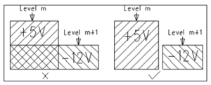
Different power layers should avoid spatial overlap. The main purpose is to reduce interference between different power supplies, especially between power supplies with very different voltages. The overlapping problem of power supply planes must be avoided. If it is unavoidable, an intermediate ground layer can be considered.
20H rule
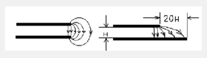 Since the electric field between the power layer and the ground layer changes, electromagnetic interference will be radiated outward at the edge of the board. called edge effect. The solution is to shrink the power layer so that the electric field is only conducted within the ground layer. Taking one H (the thickness of the medium between the power supply and the ground) as a unit, if the shrinkage is 20H, 70% of the electric field can be limited to the edge of the ground layer; if the shrinkage is 100H, 98% of the electric field can be limited within the edge.
