Shenzhen/Guangxi/Changsha

2 layers PCB
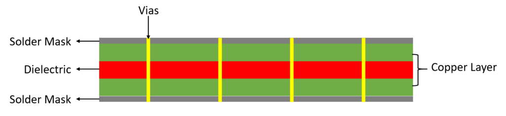
2 layers PCBs, also known as double-layer PCBs, are a type of printed circuit board that have conductive material on both sides of the insulating substrate material. This allows for more complex and compact designs compared to single-sided PCBs, as components can be placed on both sides of the board.
2 layers PCBs are widely used in various electronic applications, including industrial control, automotive, telecommunications, and medical devices. Some common applications of double-sided PCBs include:
Audio equipment: 2 layers PCBs are commonly used in audio equipment, such as amplifiers and mixers, due to their ability to accommodate complex circuit designs.
Consumer electronics: 2 layers PCBs are found in many consumer electronics products, such as smartphones, tablets, and gaming consoles, where space is limited.
Industrial equipment: 2 layers PCBs are used in various industrial applications, including motor control, machine automation, and large-scale processing operations.
Medical devices: 2 layers PCBs are used in various medical devices, such as CT scanners and ultrasound machines, where high precision and reliability are required.
Some key features of 2 layers PCBs include:
Higher circuit density: With conductive material on both sides of the board, double-sided PCBs can accommodate higher circuit densities and more complex designs compared to single-sided PCBs.
Increased design flexibility: The ability to place components on both sides of the board offers greater flexibility in designing complex circuits.
Improved signal integrity: 2 layers PCBs provide better signal routing and grounding options compared to single-sided PCBs, resulting in improved signal integrity and reduced electromagnetic interference.
Higher production costs: Due to the increased complexity of these boards, 2 layers PCBs tend to have higher production costs compared to single-sided PCBs.
In conclusion, 2 layers PCBs offer greater design flexibility, improved signal integrity, and higher circuit densities compared to single-sided PCBs. They are widely used in various electronic applications, including audio equipment, consumer electronics, industrial control, and medical devices. However, they tend to have higher production costs due to their increased complexity.
WE'RE HERE TO HELP
From engineering advice to selecting the right manufacturing partner for
you – our experience and expertise gives you the right solution.
Get in touch and let’s start working together.
Smarter PCB Solutions for Your Business: Economical, Innovative, and Efficient
Support
Office Address
Shenzhen
Guangxi
Changsha
Factory Address
Shenzhen:
F/1-3, Bldg 3, Liansheng Industiral Park, Shangxing, Shajing Town, Baoan District, Shenzhen Guangdong
Guangxi:
Building 19, Jinjiping Industrial Park, Xinping Town,
Lipu City,Guangxi
© 2026 All Rights Reserved.
