From 1+N+1 to X+N+X stack-ups, “all layer” technology and in a wide range of technological variants.
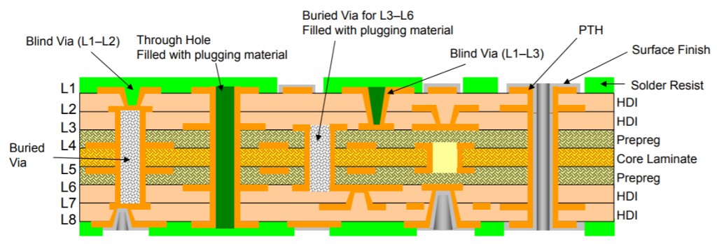
An HDI PCB is a PCB which has a far higher wiring density than a conventional through hole PCB. Per IPC-6012 (1.4.1) this is defined as a design which has an average number of electrical connections/cm² of 20 or more, on both sides of the PCB.
An HDI PCB uses finer features than a conventional PCB, enabling tighter packaging densities and lower layer count and/or reduced size. All HDI PCBs should follow IPC2226 – Sectional Design Standard for High Density Interconnect (HDI) Printed Boards. IPC2226 separates HDI into types I to type VI depending on usage and complexity.
Typical applications are smartphones, where space is at a premium, and aerospace where smaller size and/or reduced weight are key drivers.
WE'RE HERE TO HELP
From engineering advice to selecting the right manufacturing partner for you – our experience and expertise gives you the right solution.
Imagine your printed circuit board cost reduced by 30%
Get a quote now and we'll show you our proven approach to helping businesses like yours save on PCB/PCBA manufacturing costs while delivering superior products
Days
Hours
Minutes
Seconds
Get Free Samples Now
You can get the quota for free samples of 2 layer and 4 layer from our sales. Upload Gerber Files– EQ(1-2 hours)–Production(3-4 days)–ship(5-7days) . Then,free samples will in your hand. After sending the file, please pay attention to the email from our sales in 1-2 hours.