
PCB novices will always encounter various “pits” at the beginning, such as common spacing issues: the spacing between wires, the spacing between pads, etc. In this article, 2PCB will talk to you about the safety spacing issue in PCB design.
Electrical safety distance
1. Spacing between wires
This spacing needs to consider the production capacity of the PCB manufacturer. It is recommended that the spacing between traces should not be less than 4mil. The minimum line spacing is also the line-to-line and line-to-pad spacing. So, from our production perspective, of course, the bigger the better if conditions permit. Generally, the conventional 10mil is more common.
2. Pad aperture and pad width
According to PCB manufacturers, if the pad aperture is mechanically drilled, the minimum diameter should not be less than 0.2mm. If laser drilling is used, it is recommended that the minimum diameter be not less than 4mil. The aperture tolerance varies slightly depending on the board material. It can generally be controlled within 0.05mm, and the minimum pad width must not be lower than 0.2mm.
3. The spacing between pads
According to the processing capabilities of the PCB manufacturer, it is recommended that the distance between pads should not be less than 0.2mm.
4. The distance between the copper sheet and the edge of the board
The distance between the live copper sheet and the edge of the PCB is preferably no less than 0.3mm. If copper is laid on a large area, there is usually a shrinkage distance from the edge of the board, which is generally set to 20mil.
Non-electrical safety distances
1. Character width, height and spacing
Regarding silk screen characters, we generally use conventional values such as: 5/30 6/36 mil, etc. Because when the text is too small, it will be blurry when printed.
2. The distance from silk screen to solder pad
Silk screen printing is not allowed to cover the soldering pads, because if the silk screen covers the soldering pads, tin will not be applied to the silk screen printing area during tin application, thus affecting the mounting of components.
Generally, board manufacturers require a spacing of 8mil. If the area of some PCB boards is really close, the spacing of 4mil is barely acceptable. Then, if the silk screen accidentally covers the pad during design, the board manufacturer will automatically eliminate the part of the silk screen left on the pad during manufacturing to ensure that the pad is tinned. So we need to pay attention to it.
3. 3D height and horizontal spacing on the mechanical structure
When mounting components on the PCB, consider whether they will conflict with other mechanical structures in the horizontal direction and height. Therefore, when designing, it is necessary to fully consider the adaptability of the spatial structure between components, as well as between the finished PCB and the product shell, and reserve a safe distance for each target object.
Some safety distance rules
1) The spacing setting of the high voltage network must meet the regulations of the -48V power input port: the creepage distance and electrical clearance from the -48V power supply to other circuits except PGND is greater than 2.0mm; the creepage distance and electrical clearance from PGND to other circuits is greater than 2.0mm .
2) The recommended line width/space for PCB processing is: 6mil/6mil; the minimum usable line width/space is: 4mil/5mil;
Limit minimum line width/space: 4mil/4mil.
3) The green oil bridge must be no less than 2mil (except for surface mount pin-dense chips such as QFP packages), otherwise it is easy to cause tin connection between the pads during processing. The recommended settings for hole rules are as follows:
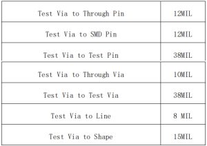
The distance between the ICT test hole Test via (the pad is 32MIL) and the pin, test pin, test via, and thru pin is set.
must be less than the following settings:
Test point spacing requirements
a) The center distance d between two test points: 85mil is best; 70mil is accepted; try to avoid 50mil.
b) The distance d between the test point and the via hole: 20mil at best; 12mil at minimum.
c) The distance between the test points and the bottom device pads d: 20mil at best; 12mil at minimum. For single boards that have undergone wave soldering, 40mil is the best; 25mil is the minimum.
d) The distance d between the test point and the solder surface trace: preferably 20mil; minimum 12mil.
e) The distance d between the test point and the edge of the PCB board: minimum 125mil. This requirement is only required for sealing ring fixtures.
f) The distance d between the test point and the positioning hole: preferably 200mil; minimum 125mil. Easy to install positioning posts.
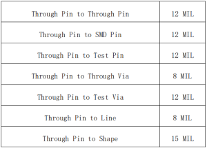
The spacing setting from Thru pin to Thru pin, SMD Pin, and Test pin must not be less than the following settings, and must also meet
SMD device layout requirements, THD layout requirements and crimp device layout requirements.
(The above spacing rules come from: a Fortune 500 company’s internal PCB design specifications)
