
The work done by PCB Layout engineers is a technical job, and it is also a meticulous job. It not only requires excellent skills, but also requires engineers to be careful and patient. In the PCB design process, because there are many rules that need to be followed, some details are often easily overlooked.
1. Placement direction and distance of components on the edge of PCB board
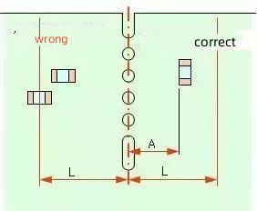
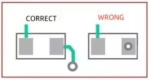
Since PCBs are generally made of panels, the devices near the edges need to meet two conditions:1) Parallel to the cutting direction to make the mechanical stress of the device uniform. If placed as shown on the left side of the picture above, when the board is to be disassembled, the two pads of the patch may be stressed in different directions, causing the components and pads to fall off.
2) Components cannot be arranged within a certain distance to prevent components from being damaged when cutting the board.
2. The ambient temperature of the electrolytic capacitor must be considered and kept away from heat sources
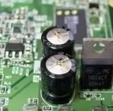
When designing, PCB engineers must first consider whether the ambient temperature of the electrolytic capacitor meets the requirements, and secondly, keep the capacitor as far away from the heating area as possible to prevent the liquid electrolyte inside the electrolytic capacitor from drying out.
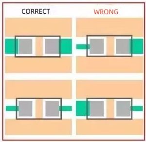
3. If the solder pad falls in a common area, heat dissipation needs to be considered
If the pad falls in the paving area, the right method should be used to connect the pad and the paving, and whether to connect 1 wire or 4 wires is determined based on the current size; if the left method is used, the components should be removed during welding or repair. It is more difficult because the temperature is completely dispersed through the copper paving, resulting in failure to solder.
4. Spacing between patches
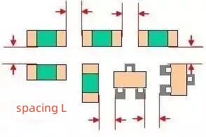
The spacing between chip components is an issue that engineers must pay attention to during layout. If the spacing is too small, it will be very difficult to print solder paste and avoid soldering. Distance recommendations are as follows:
Device distance requirements between patches:
Similar devices: ≥0.3mm
Heterogeneous devices: ≥0.13*h+0.3mm (h is the maximum height difference of surrounding nearby components)
The distance requirement between components that can only be mounted manually is: ≥1.5mm.
The above suggestions are for reference only and can be based on the respective company’s PCB process design specifications.
5. It is best not to drill through holes on the pads
Note that it is best not to drill the through holes on the pads, as this can easily cause tin leakage and false soldering.
6. The width of the leads on both sides of the component pad should be the same.
As shown in the picture above, the lead width on both sides of the component pad should be consistent.
7. If the lead is smaller than the plug-in pad, teardrops need to be added.
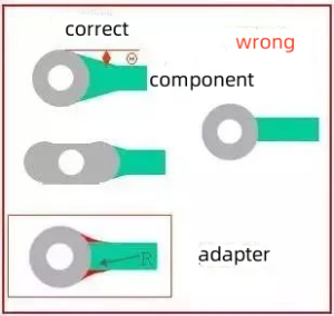
If the wire is smaller than the pad of the direct plug device, you need to add teardrops (as shown in the picture above). Adding teardrops has the following benefits:
1) Avoid reflection caused by a sudden reduction in signal line width, and smooth the transition between the wiring and component pads.
2) Solve the problem that the connection between the pad and the trace is easily broken by impact force.
3) Setting teardrops can also make the PCB circuit board look more beautiful.
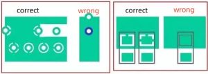
8. Pay attention to keep the pads of unused pins and connect them to ground.
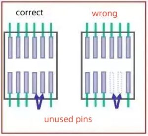
Be careful to keep the pads of unused pins and connect them to ground properly. For example, in the picture above, a chip has two pins that are not used, but the physical pins of the chip do exist. If the two pins are left floating as shown on the right side of the picture above, it is easy to cause interference. If you add a pad and ground the pad to shield it, you can avoid interference.
Whether you are a veteran or a beginner in PCB design, everyone should pay attention to the above layout details~
