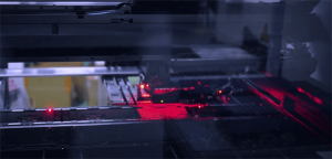
PCB manufacturing is the conversion of a circuit board design that meets design specifications into a physical PCB. Outsourcing is usually done by a contract manufacturer (CM) who strictly follows the specifications provided by the designer. Certain key factors (such as PCB substrate selection, layout strategy, surface coating requirements) are determined prior to manufacturing and may impact manufacturing yield and product performance. Therefore, understanding the PCB manufacturing process and its trends is very important for any PCB designer and manufacturer.
The growing demand for digitalization in consumer and industrial electronics has driven many innovations in the PCB manufacturing process. Advanced PCB substrate materials such as epoxy resin and polyamide meet the development needs of the global PCB market. The recycling of PCBs is now receiving widespread attention to meet environmental and sustainability guidelines set by government authorities.
The communications and automotive industries are the major applications driving the global PCB market. Technologies such as artificial intelligence, the Internet of Things, and 5G mobile communications have also impacted PCB manufacturers, bringing about a revolution in PCB design and manufacturing technology. We’ll take a look at the latest PCB design and manufacturing trends.
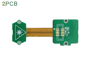
One of the rapidly growing trends in PCB manufacturing is the use of flexible PCBs because they can be transformed into any shape or size. Advantages of flexible PCBs include smaller size, greater flexibility and a variety of substrate options. These properties make them best suited to the requirements of medical, wearable and other specific applications. In addition to Flex PCBs, there are also Rigid-flex PCBs for compact product development.
Automation in every field has led to increased demand for high-density interconnect (HDI) PCBs as they provide reliable and high-speed signal transmission. HDI PCBs offer smaller trace widths, thereby increasing routing density. The reduced number of PCB layers also reduces production costs. Therefore, HDI PCBs are crucial in smart applications such as aerospace, medical and wearable technology devices.
With the focus on renewable energy sources such as solar energy, the demand for high-power PCBs is growing significantly. Most solar panels operate from a voltage range of 24 V to 48 V. In addition, electric vehicles have also increased the requirements for high-power boards. Accommodating long-lasting battery packs will allow products to run longer, requiring high-power circuit board designs with efficient heat dissipation.
PCB design technology also optimizes efficiency by introducing automatic placers and automatic routers into EDA tools. This automation is speeding up design time to market and improving quality. Going forward, CAD systems will be integrated with processes to increase the speed of design and simulation.
With the trend of connecting smartphones to smart homes or smart offices, the demand for smart devices continues to grow. Such applications require scalable and securely connected devices. This could be a huge revenue stream in the future, thus requiring PCB manufacturers to be flexible and adaptable to capture the market.
These are off-the-shelf products for commercial applications that are fully or partially designed and assembled to speed up the design process and provide other benefits. Because they comply with strict standardization and regulatory guidelines, they are an excellent choice for critical and space-based systems. Additionally, they provide reliability and efficiency with low overhead. The aerospace industry uses COTS components extensively, and other areas may soon catch up.
Control As new applications emerge, there are many opportunities to introduce new components. There is a growing need to avoid counterfeit components from the supply chain. This is necessary for critical applications such as medical devices, artificial intelligence, and virtual reality. New PCB manufacturing methods are needed to control this problem, such as implanting a microchip inside the component to protect against counterfeiting.
IoT devices are compact, portable, and reliable, prompting PCB manufacturers to implement security features to prevent tampering. IoT PCBs must adhere to specific standards and regulations to comply with the required security.
It is difficult to treat traditional PCB harmlessly because it contains a large number of non-degradable chemicals. Waste PCBs contribute to e-waste, increasing global concern about e-waste management. Biodegradable PCBs are key to solving this problem, and PCB scrap metal recycling is also needed.
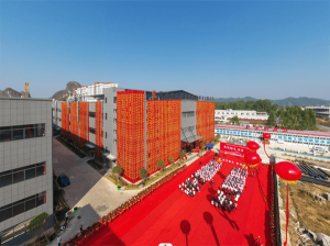
2PCB, founded in 2012, focuses on circuit board prototype manufacturing and mass production. It has high-end prototypes and rapid delivery capabilities for large, medium and small batches. Through full value chain services such as PCB production, BOM procurement and circuit board mounting, we provide vertically integrated one-stop solutions for customers’ products. We continue to contribute to the sustained innovation and development of China’s electronic technology and build a first-class electronic product design and manufacturing outsourcing service provider. Pursue the material and spiritual happiness of all employees and contribute to the progress and development of mankind and society.
We provide professional design solutions covering all aspects of PCB and PCBA layout, including the following services.
include:
1.PCB manufacturing: PCB board manufacturing capacity 1-36 layers, HDI,
2.Single-sided, double-sided, multi-layer boards, FLEX, RIGID, FLEX-RIGID, IC carrier boards
3. Quiketurn -48 hours service
4.Component procurement: BOM procurement, as fast as 3 days
5.PCB assembly: Expedited sample and batch mounting processing, only 1-3 days
6.Functional testing
7.Electronic assembly global logistics